- 您现在的位置:买卖IC网 > Sheet目录223 > ESD11B5.0ST5G (ON Semiconductor)TVS BIDIR 250MW 5V DSN2
�� �
�
�ESD11B�
�The� following� is� taken� from� Application� Note�
�AND8398/D� ?� Board� Level� Application� Note� for� 0201�
�DSN2� Package.�
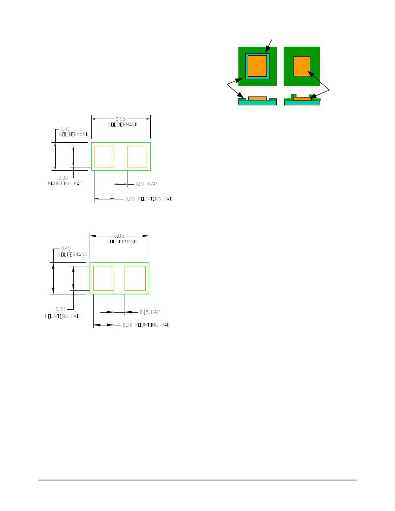
�Printed� Circuit� Board� Solder� Pad� Design�
�Solder� Mask� Openings�
�Based� on� results� of� board� mount� testing,� ON�
�Semiconductor’s� recommended� mounting� pads� and� solder�
�mask� opening� are� shown� in� Figure� 6.� Maximum� acceptable�
�PCB� mounting� pads� and� solder� mask� opening� are� shown� in�
�Solder�
�Mask�
�Overlay�
�Solderable�
�PCB�
�Figure� 7.�
�Figure� 6.� Recommended� Mounting� Pattern�
�Figure� 7.� Maximum� Recommended� Mounting�
�Solder� Mask�
�Two� types� of� PCB� solder� mask� openings� commonly� used�
�for� surface� mount� leadless� style� packages� are:�
�1.� Non� Solder� Masked� Defined� (NSMD)�
�2.� Solder� Masked� Defined� (SMD)�
�The� solder� mask� is� pulled� away� from� the� solderable�
�metallization� for� NSMD� pads,� while� the� solder� mask�
�overlaps� the� edge� of� the� metallization� for� SMD� pads� as�
�shown� in� Figure� 8.� For� SMD� pads,� the� solder� mask� restricts�
�the� flow� of� solder� paste� on� the� top� of� the� metallization� and�
�prevents� the� solder� from� flowing� down� the� side� of� the� metal�
�pad.� This� is� different� from� the� NSMD� configuration� where�
�the� solder� flows� both� across� the� top� and� down� the� sides� of� the�
�NSMD� SMD�
�Figure� 8.� Comparison� of� NSMD� vs.� SMD� Pads�
�Typically,� NSMD� pads� are� preferred� over� SMD� pads.� It� is�
�easier� to� define� and� control� the� location� and� size� of� copper�
�pad� verses� the� solder� mask� opening.� This� is� because� the�
�copper� etch� process� capability� has� a� tighter� tolerance� than�
�that� of� the� solder� mask� process.� NSMD� pads� also� allow� for�
�easier� visual� inspection� of� the� solder� fillet.�
�Many� PCB� designs� include� a� solder� mask� web� between�
�mounting� pads� to� prevent� solder� bridging.� For� this� package,�
�testing� has� shown� that� the� solder� mask� web� can� cause�
�package� tilting� during� the� board� mount� process.� Thus,� a�
�solder� mask� web� is� not� recommended.�
�PCB� Solderable� Metallization�
�There� are� currently� three� common� solderable� coatings�
�which� are� used� for� PCB� surface� mount� devices-� OSP,�
�ENiAu,� and� HASL.�
�The� first� coating� consists� of� an� Organic� Solderability�
�Protectant� (OSP)� applied� over� the� bare� copper� features.� OSP�
�coating� assists� in� reducing� oxidation� in� order� to� preserve� the�
�copper� metallization� for� soldering.� It� allows� for� multiple�
�passes� through� reflow� ovens� without� degradation� of�
�solderability.� The� OSP� coating� is� dissolved� by� the� flux� when�
�solder� paste� is� applied� to� the� metal� features.� Coating�
�thickness� recommended� by� OSP� manufacturers� is� between�
�0.25� and� 0.35� microns.�
�The� second� coating� is� plated� electroless� nickel/immersion�
�gold� over� the� copper� pad.� The� thickness� of� the� electroless�
�nickel� layer� is� determined� by� the� allowable� internal� material�
�stresses� and� the� temperature� excursions� the� board� will� be�
�subjected� to� throughout� its� lifetime.� Even� though� the� gold�
�metallization� is� typically� a� self-limiting� process,� the�
�thickness� should� be� at� least� 0.05� m� m� thick,� but� not� consist� of�
�more� than� 5%� of� the� overall� solder� volume.� Excessive� gold�
�in� the� solder� joint� can� create� gold� embrittlement.� This� may�
�affect� the� reliability� of� the� joint.�
�The� third� is� a� tin-lead� coating,� commonly� called� Hot� Air�
�Solder� Level� (HASL).� This� type� of� PCB� pad� finish� is� not�
�recommended� for� this� type� packages.� The� major� issue� is� the�
�inability� to� consistently� control� the� amount� of� solder� coating�
�applied� to� each� pad.� This� results� in� dome-shaped� pads� of�
�various� heights.� As� the� industry� moves� to� finer� and� finer�
�pitch,� solder� bridging� between� mounting� pads� becomes� a�
�common� problem� when� using� this� coating.�
�PCB� metallization.�
�http://onsemi.com�
�4�
�发布紧急采购,3分钟左右您将得到回复。
相关PDF资料
ESD11L5.0DT5G
TVS ESD UNIDIRECT 150MW SOT-1123
ESD11N5.0ST5G
TVS BIDIR 250MW 5V DSN2
ESD1P0RFWE6327
DIODE RF ESD 1CH SOT323
ESD3V3U1U-02LS E6327
DIODE TVS 3.3V TSSLP-2-1
ESD3V3U4ULC E6327
DIODE TVS 3.3V TSLP-9-1
ESD4238MTTAG
IC ESD CLAMP ARRAY 8CH 16-WDFN
ESD5384NCTBG
DIODE ESD PROTECT 4CH 9-WLCSP
ESD5B5.0ST1G
TVS BIDIRECT 50W SOD523
相关代理商/技术参数
ESD11H120
制造商:Panasonic Industrial Company 功能描述:SWITCH
ESD11L5.0DT5G
功能描述:TVS二极管阵列 LO CAP ESD PROT 5.0V RoHS:否 制造商:Littelfuse 极性: 通道:4 Channels 击穿电压: 钳位电压:11.5 V 工作电压:2.5 V 峰值浪涌电流:20 A 安装风格:SMD/SMT 端接类型:SMD/SMT 系列: 最小工作温度:- 40 C 最大工作温度:+ 85 C
ESD11N5.0ST5G
功能描述:TVS 二极管 - 瞬态电压抑制器 LOW CAP BI DIRECT TV RoHS:否 制造商:Vishay Semiconductors 极性:Bidirectional 工作电压: 击穿电压:58.9 V 钳位电压:77.4 V 峰值浪涌电流:38.8 A 系列: 封装 / 箱体:DO-214AB 最小工作温度:- 55 C 最大工作温度:+ 150 C
ESD11V120
制造商:Panasonic Industrial Company 功能描述:SWITCH
ESD11V130
制造商:Panasonic Industrial Company 功能描述:SWITCH
ESD11V220
制造商:Panasonic Industrial Company 功能描述:SWITCH
ESD11V220K
制造商:Panasonic Industrial Company 功能描述:SWITCH
ESD11V230
制造商:Panasonic Industrial Company 功能描述:SWITCH